Nanosecond UV & Green Laser Cutting for PCB and FPC
Nanosecond UV & Green Laser Cutting for PCB and FPC
Clean edges, tight tolerances, and factory-grade throughput with AONano Precision UV & GR
Why lasers for PCB/FPC cutting?
Modern electronics demand smaller footprints, tighter panelization, and materials that don’t love mechanical tools. Traditional de-paneling, routers, punches/dies, or V-scoring—can leave burrs, dust, micro-cracks, and mechanical stress that lower yield and reliability. Nanosecond UV and Green lasers deliver non-contact, programmable cutting with minimal heat, enabling precise singulation for rigid PCBs and flexible circuits.
Key benefits vs. mechanical/CO₂/IR:
Low HAZ, low burr edges on FR-4, polyimide (PI), adhesives, and coverlay
Tight contours & micro-features (slots, small radii, internal windows)
No tooling cost; instant recipe changes for new outlines
Less charring than IR/CO₂ on organics; better copper interaction than UV-only
High repeatability—ideal for camera modules, wearables, medical electronics
UV vs. Green: when to use which?
Different PCB stacks absorb laser light differently. Using the right wavelength (or a hybrid recipe) is what turns “good” into “production-ready.”
Stronger interaction with metals (copper) and many composites
Improves edge cleanliness where copper planes or heavier copper dominate
Great for FR-4 depaneling, mixed-stack cuts, and copper-rich zones
Pro tip: Many factories run UV-led passes for polymer layers and Green passes at lower fluence for copper edges, delivering cleaner multi-layer results and faster cycle times.
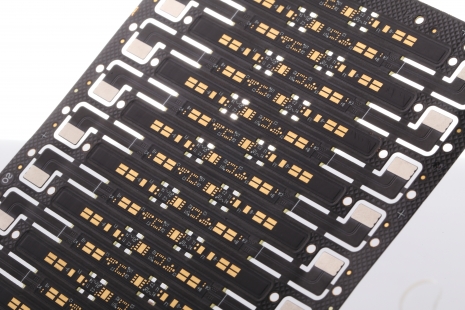
Common applications
De-paneling / Singulation of rigid FR-4 and flexible PI circuits
Coverlay, stiffener, and adhesive cutting (FPC assembly)
Internal windows & slots for sensors, buttons, and optical paths
Connector fingers & fine tabs with small fillets for stress relief
Final outline tuning after SMT (with vision-assisted registration)
Materials supported: FR-4, polyimide (PI), adhesive tapes/PSA, coverlay, PET (with proper fixturing), aluminum-backed substrates (careful fixturing/recipes), copper foils and laminates. Higher absorption on Cu, Au, and ceramics at 532 nm.
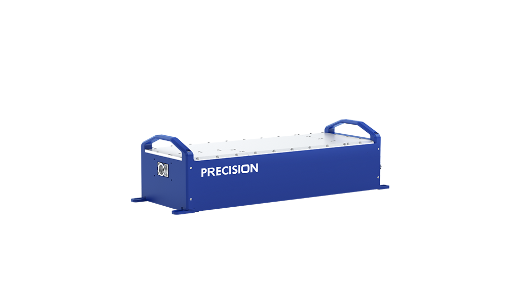
AONano Precision UV & GR — built for production
AOC’s high-power AONano Precision UV (355 nm) and AONano Precision GR (532 nm) nanosecond lasers are engineered for 24/7 electronics manufacturing:
High average power & peak power for fast scan speeds and narrow kerfs
Excellent beam quality (low M²) for small spots and clean edges
Flexible repetition rates to balance throughput and edge integrity
Seamless integration with galvo scanners, vision alignment, and motion stages
Industrial reliability with long lifetime optics and stable power over shifts
Outcome: Clean, consistent depaneling with reduced rework and higher yield—without the tooling cost and dust of routers.