


SOLUTIONS

Consumer Electronics
The consumer electronics market is responsible for the recent explosion of new materials that have made it into real world products. The influx of new materials and the ever-changing requirement to make our consumer products smaller with additional functions and features has presented the manufacturing world with a lot of new challenges. These challenges have proven difficult or seemingly impossible to resolve with traditional manufacturing technologies.
View Details

New Energy
Recent development in laser technology and optical instruments enables new processes and technologies in the energy industry. Laser processing provides several advantages over the conventional processes includes precision of operation, local treatment, fast processing, and low cost. Shaping the energy materials is one of the major applications in laser processing, includes net shaping of thermoelectric pins, scribing of thin-film solar cells, edge isolation of crystalline silicon solar cells, laser doping of solar cells, surface texturing for hydrophobicity, and photon capturing.
• Scribing
• Texturing
• Doping
• Surface alloying
• Net shaping
• Scribing
• Texturing
• Doping
• Surface alloying
• Net shaping
View Details
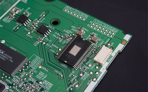
PCB
Laser processing in the printed circuit board (PCB) industry is seen as critical in technological advancement with cutting-edge innovation that ensures practical and stylish electronic devices. It offers significant benefits in this context in terms of laser PCB depaneling, laser PCB drilling, laser marking.
• High cutting edge quality
• Stress-free, dust-free processing
• Material diversity, rigid, flexible, metallic and ceramic
• Shape design freedom
• High cutting edge quality
• Stress-free, dust-free processing
• Material diversity, rigid, flexible, metallic and ceramic
• Shape design freedom
View Details
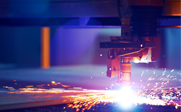
Metal Processing
Laser technology offers several advantages over traditional methods, such as precision, speed, versatility, and minimal heat-affected zones. Common laser processing of metal includes: cutting, welding, drilling, engraving, marking, etc.
View Details


